
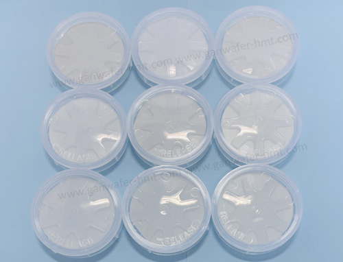
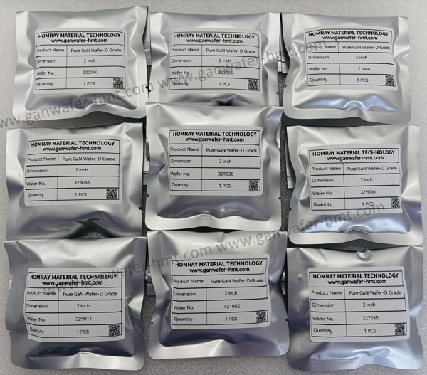
2 Inch Pure GaN Wafer Supplier
Dimensions: Ф 50.8 mm ± 0.5 mm
Thickness:400 ± 25 µm
Useable Surface Area: > 90%
Grade: D R P
Product Description
Pure GaN Wafer (Freestanding GaN Substrate Wafer)
High Quality Freestanding GaN Substrate Wafer Manufacturer
HMT is a professional Pure GaN Wafer manufacturer and supplier, providing high-quality 2 inch and 4 inch Freestanding GaN Substrate Wafers for next-generation semiconductor applications. Unlike GaN-on-sapphire templates, pure GaN wafers are self-supported gallium nitride substrates with excellent crystal quality, low defect density, and superior electrical and thermal performance.
Our Bulk GaN Wafer and Native GaN Substrate Wafer products are designed for advanced GaN-based electronic and optoelectronic devices, including high-power transistors, RF communication components, micro LED displays, laser diodes, and ultraviolet optoelectronic devices.
The basic spec of Free standing GaN Wafer:
Grade: D grade R grade and P grade
Diameter: 50.8±0.5mm
Thickness:400±25um
Orientation:c-plane(0001) off angle toward Maxis 0.35+0.15°
OF:16+1 mm (1-100)
lF:8±1 mm (11-20)
Ga face:RMS <0.3 nm(10x10um)
Resistivity(300k): ≤0.02 Ω.cm
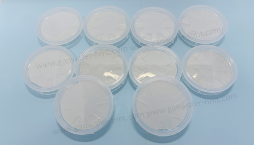
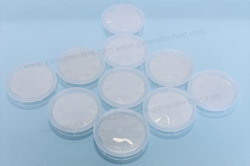
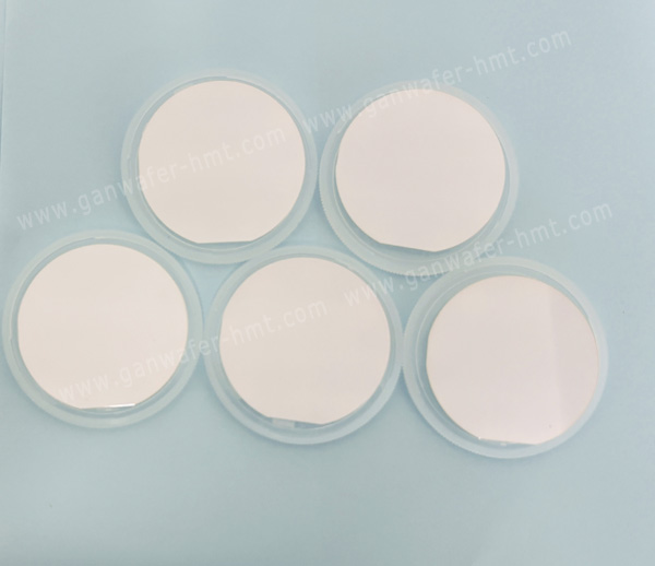
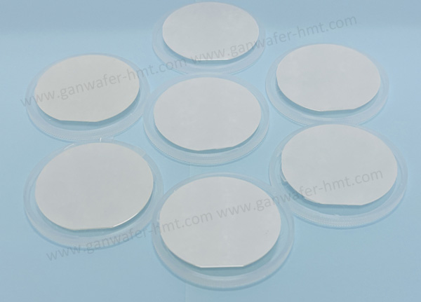
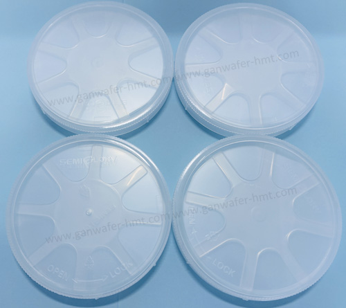
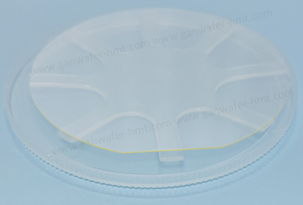
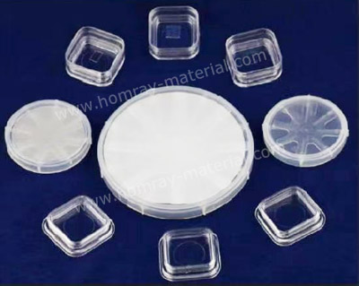
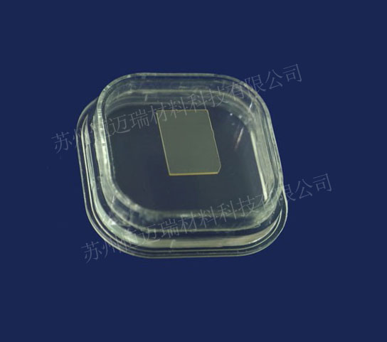
Picture of 2 inch GaN Substrate Wafers:
What is Pure GaN Wafer?
-
Lower lattice mismatch
-
Reduced threading dislocation density
-
Higher electron mobility
-
Better thermal conductivity
-
Improved device reliability
Key Features of Freestanding GaN Substrate Wafer
1. Superior Crystal Quality
High-quality GaN crystal growth technology enables low defect density and excellent crystalline performance, improving the efficiency and lifetime of GaN devices.
2. Excellent Thermal Performance
GaN material has high thermal conductivity, allowing devices to operate under high power density and high temperature conditions.
3. Low Defect Density
Freestanding GaN substrates significantly reduce crystal defects compared with heteroepitaxial GaN layers grown on sapphire.
4. High Electrical Performance
Pure GaN wafers support high electron mobility and high breakdown voltage, making them suitable for advanced power and RF applications.
5. Flexible Device Development
GaN substrates can support various epitaxial structures for electronic, RF, and optoelectronic semiconductor manufacturing.
Advantages Compared with Traditional Substrates
Freestanding GaN Wafer vs Sapphire Substrate
| Feature | Freestanding GaN Wafer |
Sapphire |
| Lattice Match | Excellent | Large mismatch |
| Defect Density | Low | Higher |
| Thermal Conductivity | High | Moderate |
| Device Performance | Superior | Limited |
| High Power Application | Excellent | Moderate |
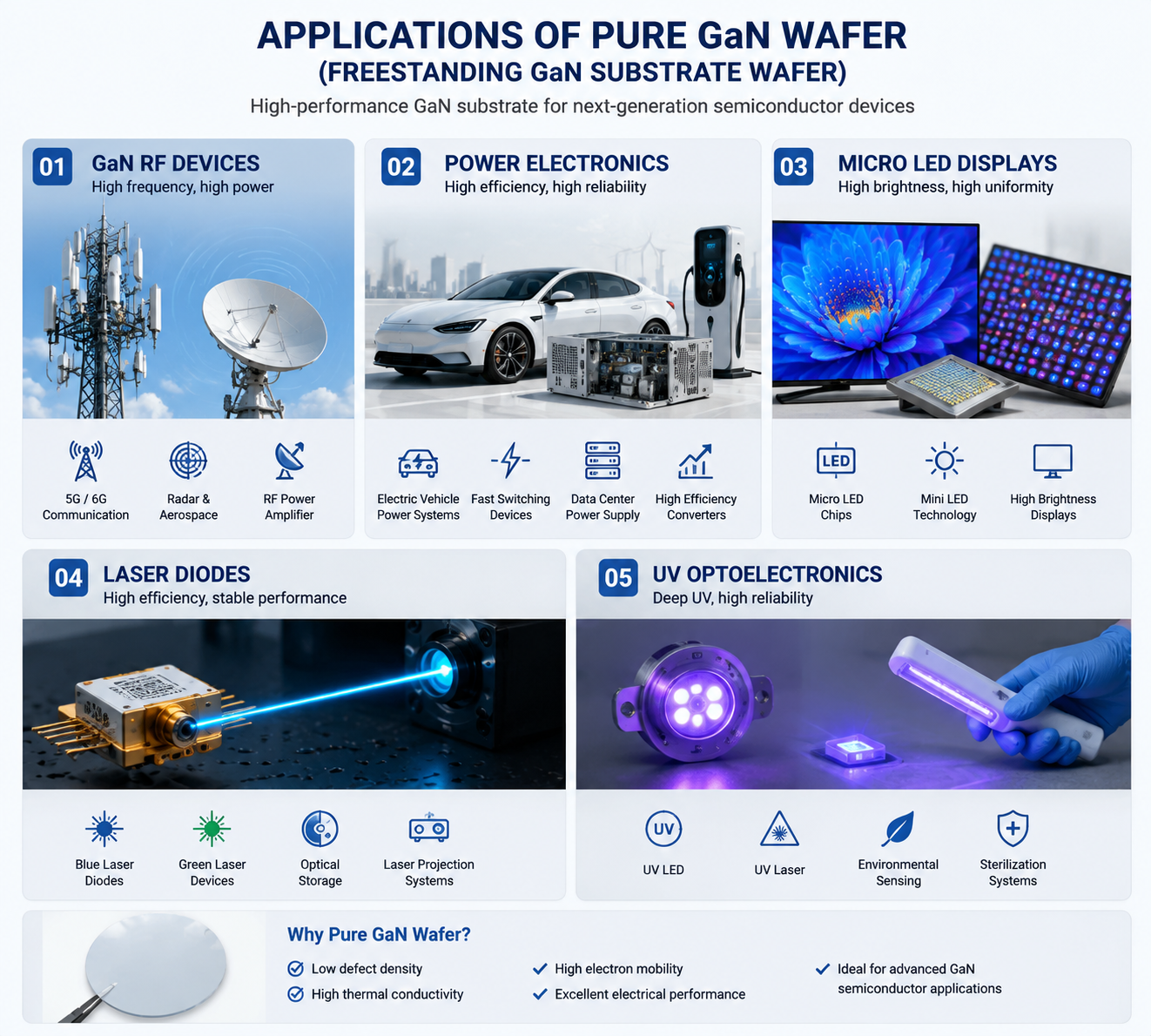
Applications of Pure GaN Wafer
1. GaN RF Devices
Freestanding GaN substrates are widely used for: GaN HEMT / RF power amplifiers / 5G communication systems / Radar and aerospace electronics
2. Power Electronics
GaN wafers enable: High voltage power transistors / Fast switching devices / EV power systems / Data center power solutions / High efficiency converters
3. Micro LED Displays
Pure GaN substrates provide excellent material quality for: Micro LED chips / Mini LED technology / High brightness displays
Related Products
 E-mail: kim@homray-material.com;tina@homray-material.com
HMT Silicon Carbide (SiC) Wafer Website: www.sicwafer-hmt.com