
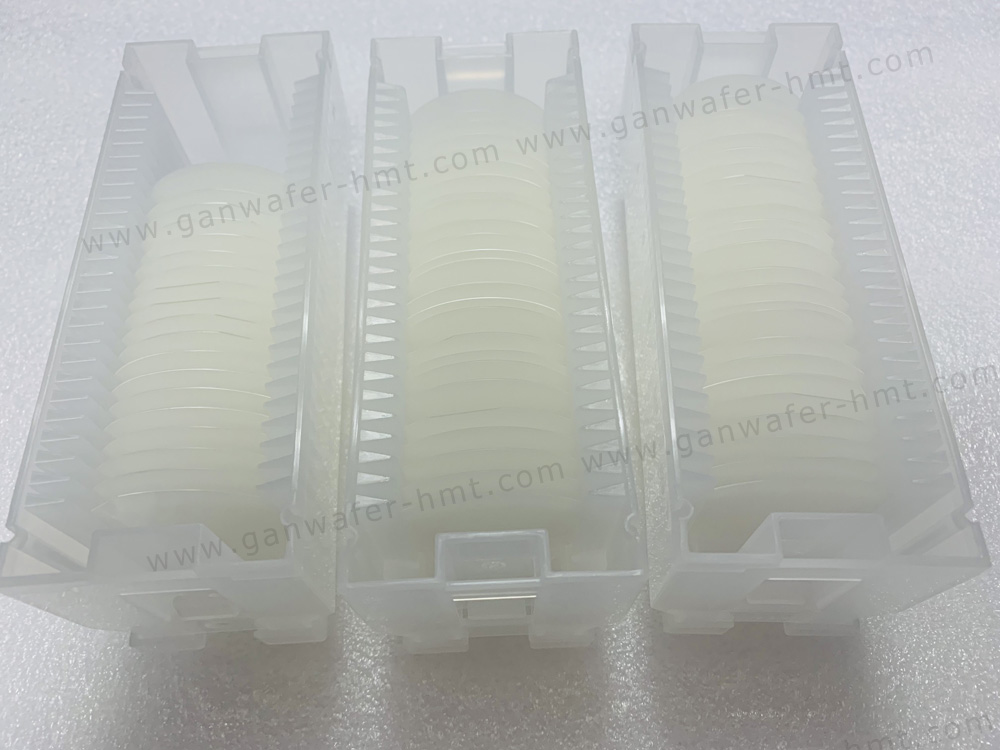

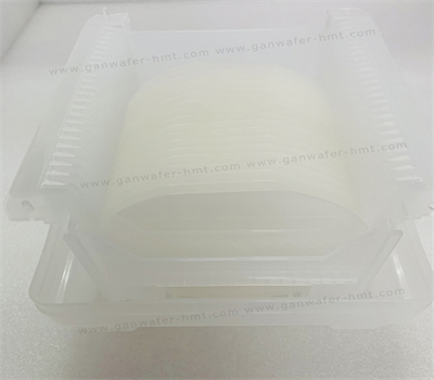
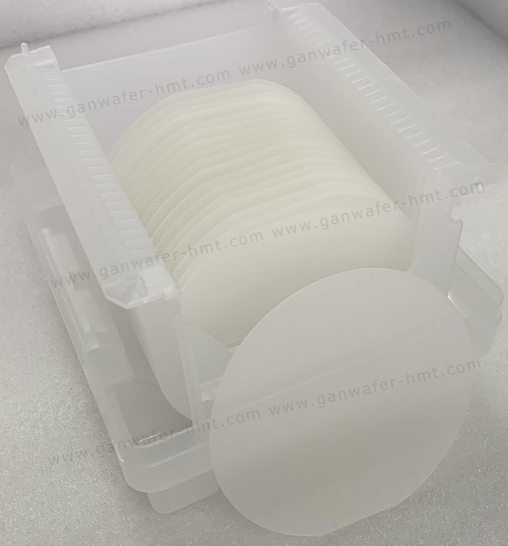
2 Inch GaN-On-Sapphire Template Wafer Manufacturer
Dimensions: Ф 50.8 mm ± 0.5 mm
Thickness:4.5µm
Orientation:C-plane(0001) A-axis 0.2± 0.1°
Useable Surface Area:> 90%
Product Description
GaN on Sapphire Template Wafer Manufacturers for Advanced Semiconductor Applications
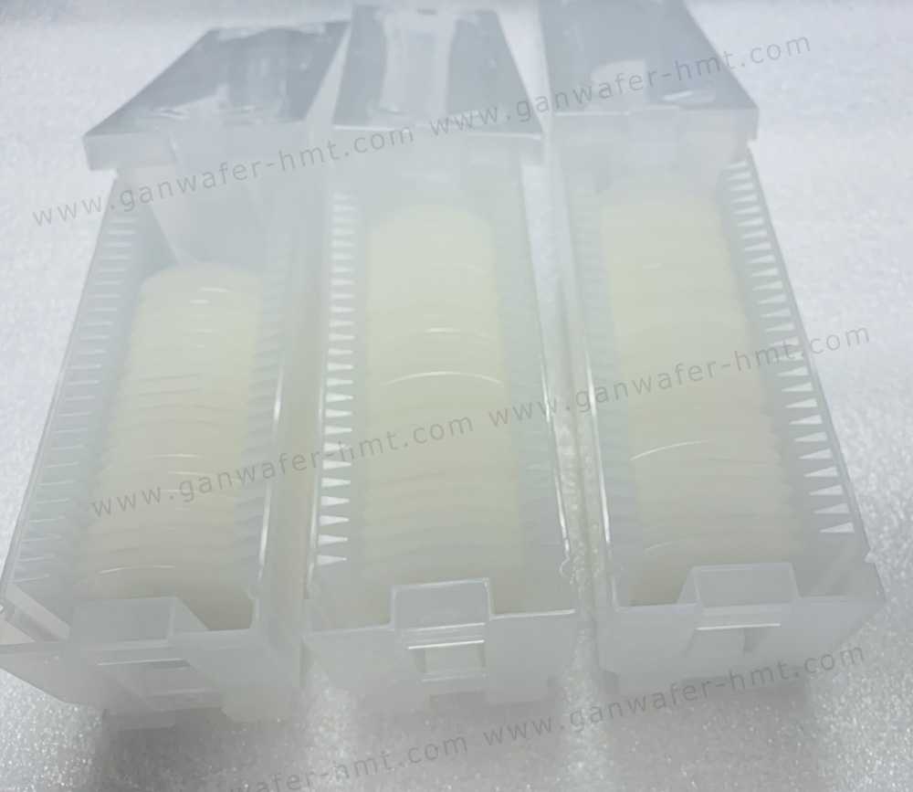
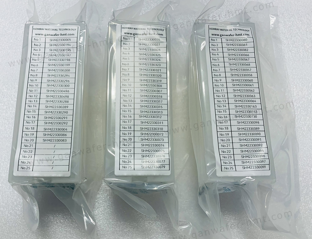
HMT is one of the professional GaN on Sapphire template wafer manufacturers specializing in high-quality gallium nitride (GaN) template wafers grown on sapphire substrates for semiconductor and optoelectronic applications. Our GaN on Sapphire template wafers include un-doped N type, Si-doped N type, both provide a reliable epitaxial platform for the development and production of GaN-based devices, including LED chips, RF devices, power electronics, laser diodes, and advanced semiconductor components.
By combining high-quality sapphire substrates with optimized GaN epitaxial layers, HMT delivers GaN template wafer solutions with excellent crystal quality, uniform thickness, and stable performance. We supply 2 inch and customized GaN on Sapphire wafers with different GaN layer thicknesses, including standard and customized specifications according to customer requirements.
As an experienced GaN wafer supplier and GaN substrate manufacturer, HMT supports global customers in research, development, and volume production of next-generation GaN semiconductor technologies.
Applications of GaN on Sapphire Wafer
LED Manufacturing
Si-doped GaN on Sapphire wafers are widely used as semiconductor platforms for blue, green, and ultraviolet LED production. The GaN epitaxial structure provides excellent optical performance and device reliability.
RF and Microwave Devices
Due to high electron mobility and high-frequency performance, GaN wafers are ideal materials for RF components, including high-power amplifiers and communication devices.
Power Electronics
GaN semiconductor materials enable the development of high-efficiency power devices with fast switching speed, low energy loss, and high voltage capability.
Semiconductor Research and Development
2 inch GaN on Sapphire wafers are commonly used in universities, laboratories, and semiconductor research centers for GaN-based device development and material studies.

Advantages of GaN on Sapphire Template Wafer
High Quality GaN Epitaxial Platform
A high-quality template substrate is essential for growing GaN epitaxial layers with improved crystal performance.
The GaN on Sapphire template wafer provides a stable foundation for GaN device fabrication and helps achieve:
- Uniform GaN layer growth
- Reliable epitaxial performance
- Reduced manufacturing complexity
- Improved device consistency
Cost-Effective Sapphire Substrate Solution
Sapphire is widely used as a GaN growth substrate because of its excellent mechanical stability, availability, and cost advantages. Compared with other GaN substrates, GaN on Sapphire wafers provide an economical solution for large-scale LED and semiconductor manufacturing.
Flexible GaN Layer Customization
HMT provides customized GaN template wafers according to different application requirements.
Customization options include:
- GaN layer thickness
- Wafer size
- Conductivity type
- Surface polishing condition
- Epitaxial structure
What sizes of GaN on Sapphire template wafers are available?
HMT provides standard 2 inch and 4 inch GaN on Sapphire template wafers, with customized sizes and specifications available according to customer requirements.
Related Products

 E-mail: kim@homray-material.com;tina@homray-material.com
HMT Silicon Carbide (SiC) Wafer Website: www.sicwafer-hmt.com