
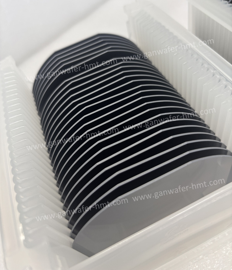
UID-GaN on Si Epi Wafer for Piezoelectric GaN Sensors
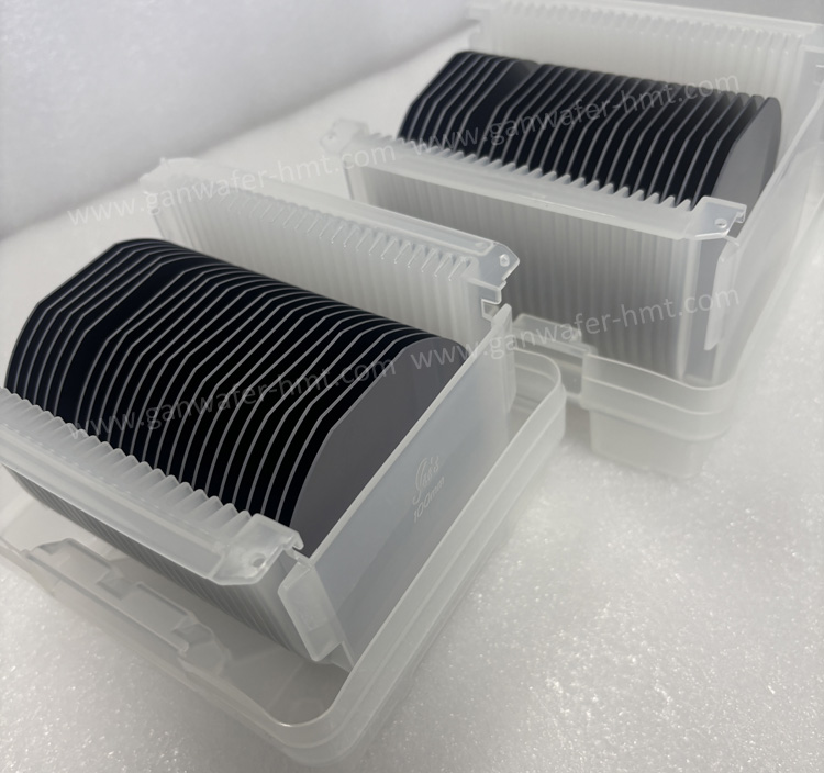
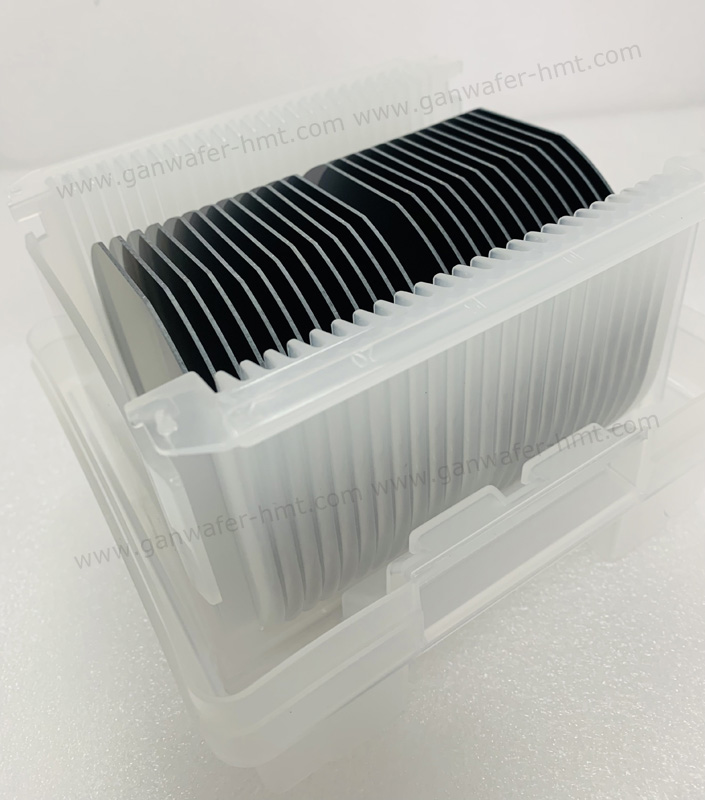
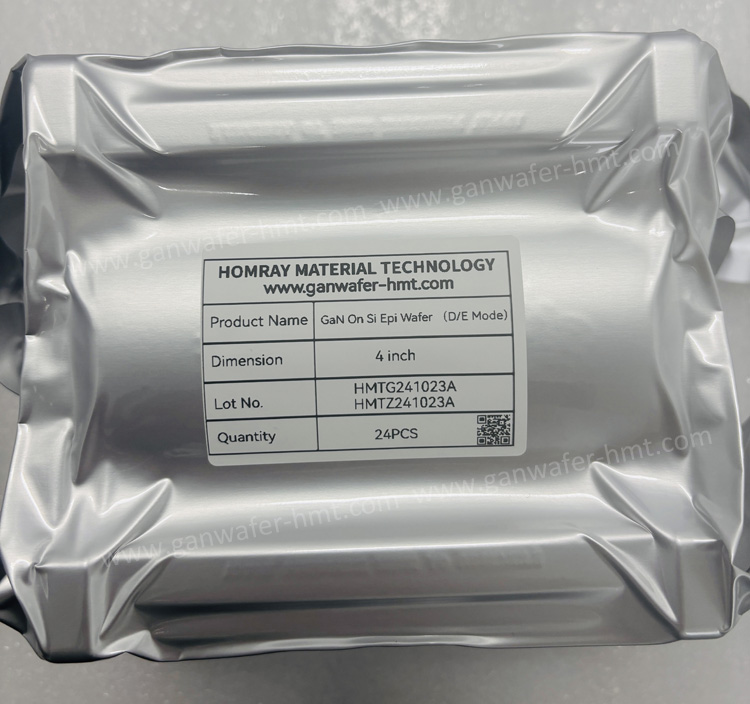
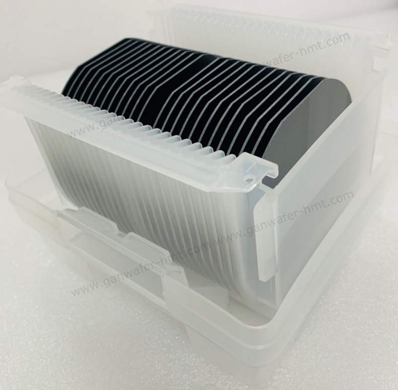
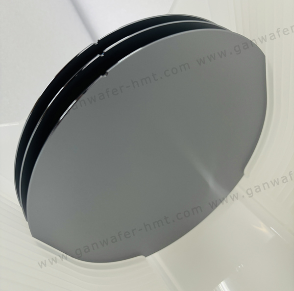
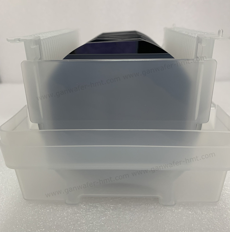
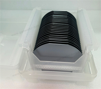
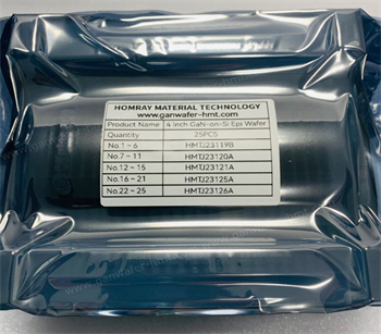
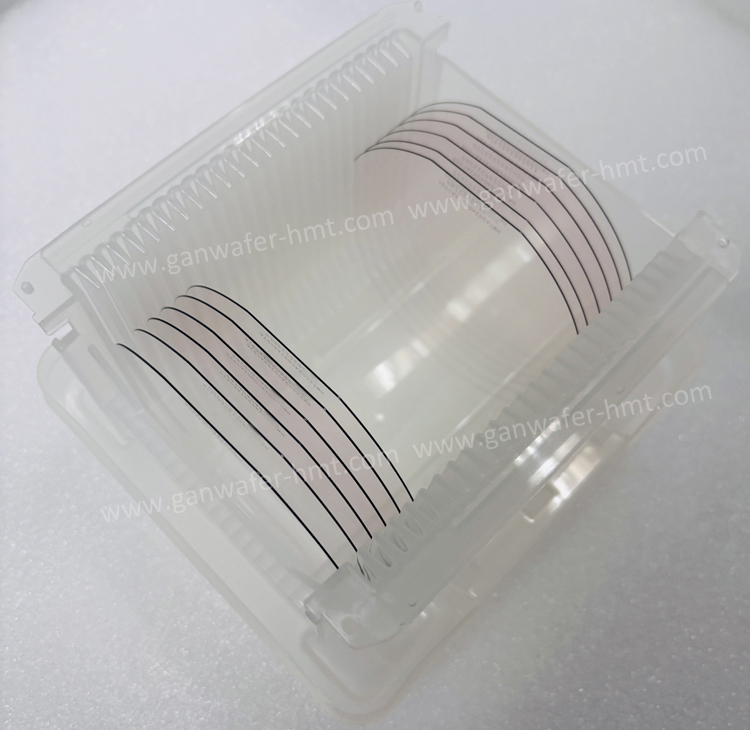
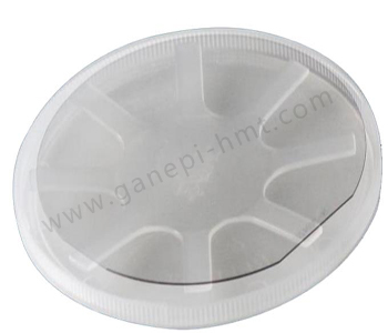
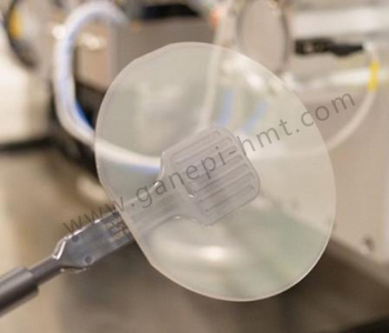
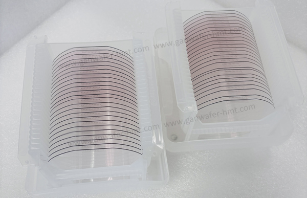
GaN-On-Si Epi Wafer
For Piezoelectric GaN Sensors
Substrate Diameter:2 inch 4 inch 6 inch 8 inch
Substrate Thickness:675um 1000um
Product Description
A GaN-on-Si Epi Platform for Strain and Pressure Sensing
HMT provides UID-GaN on Si epitaxial wafers designed as material platforms for piezoelectric GaN sensor, MEMS and electromechanical device development. The GaN surface is supplied as an epitaxial layer with no intentional dopant added to the UID-GaN layer, allowing researchers to build sensor structures around the intrinsic electromechanical properties of GaN.
GaN has a wurtzite crystal structure and exhibits piezoelectric behavior, making GaN-based thin films attractive for sensing mechanical deformation, pressure and vibration. A GaN-on-Si platform can also support wafer-level MEMS processing and suspended structures, with published research demonstrating GaN-on-Si piezosensitive devices and microsensors.
Why UID-GaN for Piezoelectric Sensing?
The sensing response of a GaN structure can be influenced by mechanical strain, crystal orientation, electrical configuration and device geometry. Using unintentionally doped GaN provides a defined starting material without intentional Si, Mg or other dopant addition to the GaN layer.
UID-GaN should be understood as a growth condition and doping configuration, rather than a claim that the material contains zero electrically active impurities. Published studies of UID-GaN report residual donor-related conductivity, so electrical specifications should be defined by measured carrier concentration, resistivity or mobility when required.
For sensor development, this distinction allows researchers to select the electrical characterization requirements independently from the intended piezoelectric device structure.
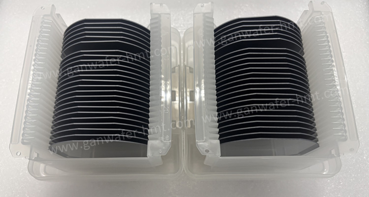
GaN-on-Si Structure for Sensor Development
The wafer can be represented as a layered starting platform:
UID-GaN Epitaxial Layer
AlGaN/AlN Buffer
Silicon (111) Substrate
The exact buffer and transition-layer design can be adjusted according to the required GaN-on-Si process. This is important because GaN and silicon have substantially different lattice and thermal-expansion characteristics, making the buffer structure an important part of GaN-on-Si epitaxy.
For sensor applications, the final stack can be designed around the intended membrane, diaphragm, resonator or strain-sensing structure rather than using a conventional HEMT stack by default.
Typical UID-GaN on Si Configuration
| Parameter | Typical Configuration |
| GaN Material | UID-GaN |
| Intentional Doping | None |
| Substrate | Silicon |
| Si Orientation | (111) |
| GaN Surface | Epi-ready |
| Application | Piezoelectric Sensor / MEMS |
| Wafer Size | 4" / 6" / 8" options subject to structure |
| GaN Thickness | Customization |
| Buffer Structure | Customization |
For wafer diameter, HMT already supplies GaN-on-Si epi wafers in 4-inch, 6-inch and 8-inch configurations across its existing product family, while the sensor-specific stack should be confirmed separately before quotation.

Applications of UID-GaN on Si Epi Wafer
Piezoelectric GaN Sensors
UID-GaN can serve as the active semiconductor material in piezoelectric sensing structures designed to detect mechanical deformation, force or pressure.
GaN MEMS
GaN-on-Si provides a wafer-level platform for developing suspended membranes, beams and other micromechanical structures. Published GaN-on-Si work has demonstrated suspended GaN MEMS structures with piezosensitive sensing elements.
Pressure Sensing
GaN-on-Si has been investigated for pressure sensors, including structures fabricated on 150 mm wafers and membrane dimensions ranging from 1 mm to 3 mm in one recent research platform.
Vibration and Acceleration Sensing
GaN's electromechanical properties can be incorporated into MEMS structures for vibration and acceleration sensing. Earlier GaN-on-Si research demonstrated a piezosensitive microaccelerometer with a 250 × 250 µm² proof-mass area.
High-Temperature Sensor Research
GaN is also investigated for sensing under elevated-temperature conditions because of its wide bandgap and thermal stability. Published GaN piezoelectric pressure-sensor research has demonstrated operation up to 350 °C, although actual operating limits depend on the complete sensor structure rather than the wafer alone.

Request a UID-GaN on Si Epi Wafer
If you are developing a piezoelectric GaN sensor, GaN MEMS device, pressure sensor or strain-sensitive structure, HMT can evaluate a UID-GaN-on-Si epi wafer based on your required device architecture.
Send your wafer size, Si orientation, UID-GaN thickness, buffer structure and epi-surface requirements to discuss a customized wafer configuration.
Sensor Concept → Epi Structure → UID-GaN Layer → MEMS Fabrication → Device Characterization
FAQ
What is a UID-GaN on Si epi wafer?
A UID-GaN on Si epi wafer is a silicon-based epitaxial wafer containing a GaN layer grown without intentional dopant addition. The platform can be used for GaN research, MEMS and piezoelectric sensor development.
For projects where sapphire rather than silicon is required as the starting substrate, see our GaN-on-Sapphire Epi Wafer options.
What does UID-GaN mean?
UID-GaN means unintentionally doped GaN, indicating that no intentional donor or acceptor dopant is added during the GaN growth process. UID-GaN can still exhibit measurable electrical conductivity due to residual impurities and native defects.
Can UID-GaN on Si be used for piezoelectric sensors?
Yes. GaN is a piezoelectric semiconductor, and GaN-on-Si platforms have been demonstrated in piezosensitive MEMS and sensor structures. Published research includes GaN-on-Si microsensors and pressure-sensing structures.
Related Products


 E-mail: kim@homray-material.com;tina@homray-material.com
HMT Silicon Carbide (SiC) Wafer Website: www.sicwafer-hmt.com