
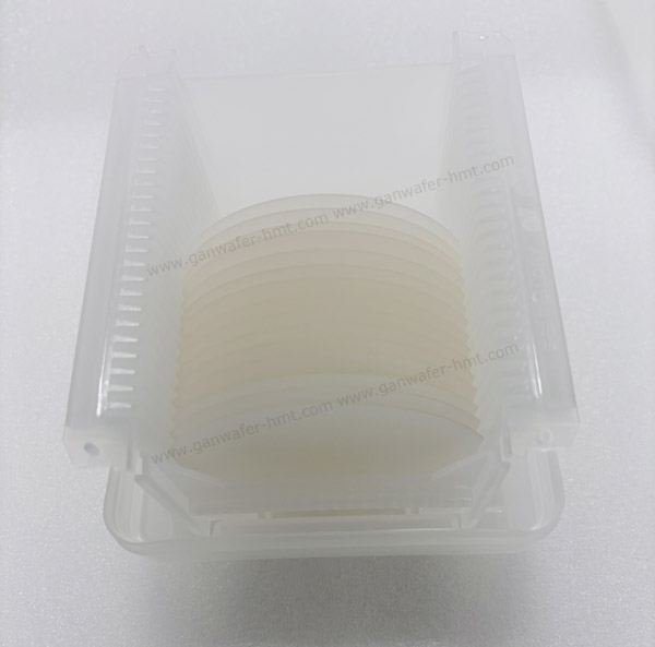
20µm Customized GaN on Sapphire Template Wafer
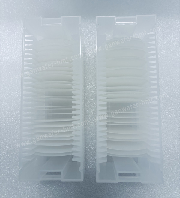
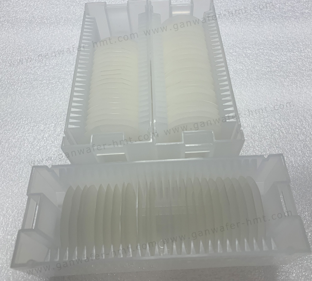
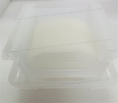
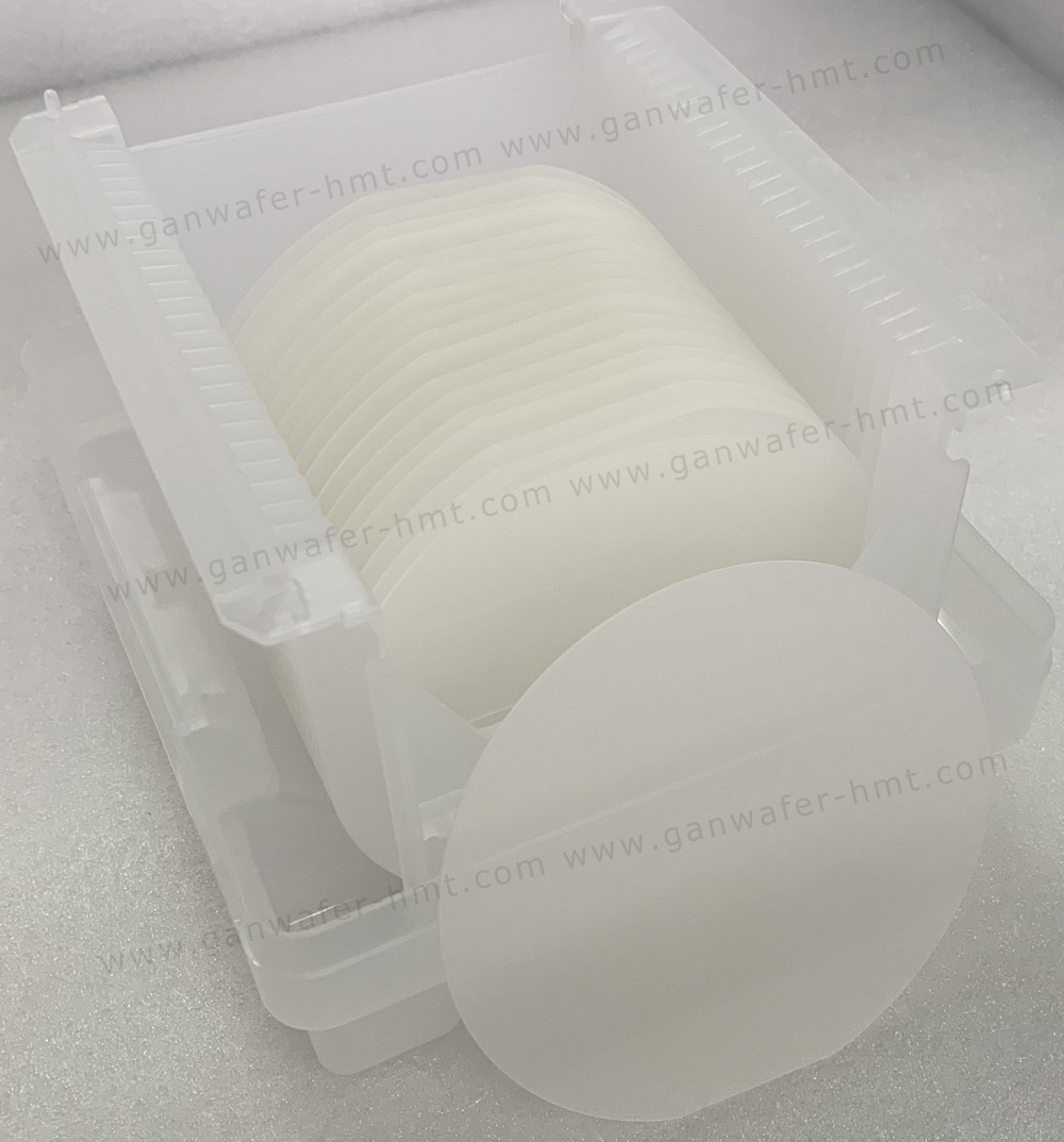
Dimensions: 2inch 4inch
Thickness:20µm
Orientation:C-plane(0001)
Useable Surface Area:> 90%
Product Description
From a 4.5 µm Standard to a Customized GaN Layer
HMT supplies GaN on Sapphire template wafers with a 4.5 µm standard GaN layer thickness, while thicker GaN layers can be customized according to project requirements. 20 µm GaN on Sapphire is available as a customized configuration for applications that require a substantially thicker GaN layer.
The template combines a GaN layer with a sapphire substrate and is typically supplied in C-plane (0001) orientation. Wafer diameter, GaN thickness, conductivity type and surface configuration can be discussed according to the intended epitaxy, research or device-development process.
Standard GaN Layer:4.5 µm
Custom GaN Layer:20 µm or Application-Specific Thickness
Wafer Formats: 2" / 4"
Substrate:C-Plane Sapphire
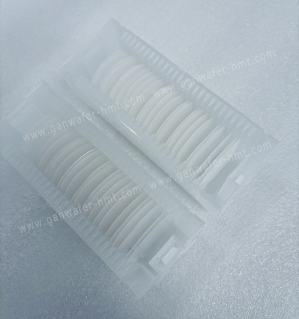
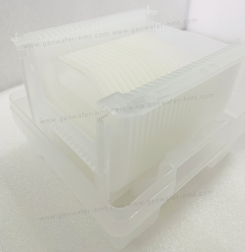
20 µm Is a Customized Thickness Option
The 4.5 µm GaN layer is the standard configuration for this template wafer family. When a project requires a thicker GaN surface layer, HMT can evaluate customized thicknesses, including 20 µm.
This distinction is important because a 20 µm GaN-on-sapphire template is not simply a different product name for the standard wafer. It represents a customized GaN layer configuration developed around a specific material, epitaxy or research requirement.
Choose the GaN Thickness Around Your Application
Different semiconductor processes can require different starting GaN layer thicknesses. A 4.5 µm template may be appropriate for one process, while another project may require a thicker GaN layer before subsequent epitaxial growth or material development.
HMT therefore offers customized GaN thickness options rather than limiting the template to a single film thickness. The 20 µm configuration can be evaluated as a customized specification together with wafer diameter, conductivity, substrate orientation and surface finish.
Build Your GaN-on-Sapphire Template
Rather than selecting a template only by wafer diameter, customers can define the main parameters of the starting structure.
| Parameter | Standard Configuration | Customization Option |
| GaN Layer Thickness | 4.5 µm | 20 µm / Other Thickness |
| Wafer Diameter | 2inch 4inch 6inch | 2inch 4inch 6inch |
| Substrate | Sapphire | Sapphire |
| Orientation | C-plane (0001) | C-plane (0001) |
| Conductivity | Undoped / Si-doped N-type | Undoped / Si-doped N-type |
| Surface | SSP / DSP | SSP / DSP |
| Template Structure | GaN on Sapphire | GaN on Sapphire |
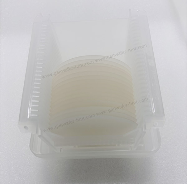 Why Customize the GaN Layer Thickness?
GaN template requirements are not identical across all research and semiconductor processes. The required starting thickness can depend on the planned epitaxial structure, material-development objective and downstream processing sequence.
A customized thickness can therefore be useful when the standard 4.5 µm configuration does not provide the desired starting layer.
Depending on the project, the template can support GaN epitaxy development, semiconductor material research, RF device research, power electronics development, optoelectronic research and laboratory process engineering.
For applications requiring a native GaN starting substrate instead of a sapphire-supported template, consider a Free-Standing GaN Substrate.
Where a 20 µm GaN Template Can Fit?
GaN Epitaxy Development
A customized 20 µm GaN layer can be considered when the planned process requires a thicker GaN starting surface before subsequent material growth.
Semiconductor Material Research
Researchers can specify the GaN thickness according to the structure they intend to investigate, making customized templates useful for controlled material experiments.
RF and Power Device Research
GaN-on-sapphire templates can serve as starting substrates for selected GaN-based electronic device development programs.
Optoelectronic Development
GaN templates can also be used in research involving GaN-based optoelectronic structures and material systems.
University and Laboratory Projects
The availability of both a 4.5 µm standard configuration and customized thicknesses such as 20 µm provides flexibility for experimental projects with different starting-layer requirements.

Request a Custom GaN Template
Need a standard 4.5 µm GaN on Sapphire template or a customized 20 µm GaN on Sapphire template wafer?
Send HMT your required wafer size, GaN thickness, conductivity type, orientation and surface configuration. We can evaluate the requested structure and discuss a customized GaN-on-sapphire template for your research or semiconductor process.
Your Requirement
Wafer Size → GaN Thickness → Conductivity → Surface → Application
FAQ
What is the standard GaN thickness?
The standard GaN layer thickness is 4.5 µm. Customized thicknesses can be evaluated when a project requires a different GaN layer configuration.
Is 20 µm GaN on sapphire available?
Yes. 20 µm is available as a customized GaN layer thickness, rather than the standard thickness of this product.
Can I order a GaN template thicker than 4.5 µm?
Yes. HMT can evaluate customized GaN layer thicknesses according to the required wafer structure, including a 20 µm configuration.
Related Products

 E-mail: kim@homray-material.com;tina@homray-material.com
HMT Silicon Carbide (SiC) Wafer Website: www.sicwafer-hmt.com