
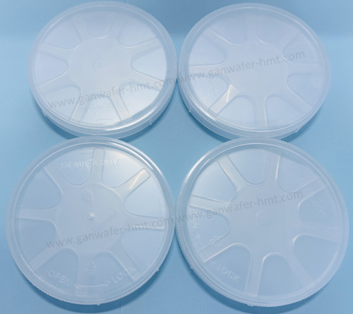
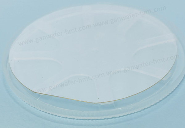
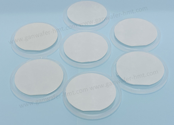
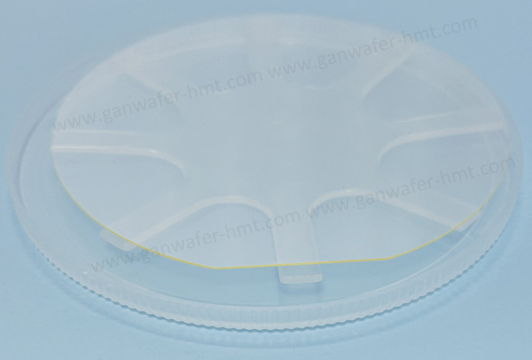
4 inch Free-Standing GaN Wafer Manufacturer
Dimensions: Ф 100 mm ± 0.3 mm
Thickness: 450 ± 30 µm
Useable Surface Area: > 90%
Grade: D R P
Product Description
Are you looking for 4 inch Free-standing GaN Wafer Manufacturer in China? Actually, HMT can produce different grades of 4 inch Free-standing GaN Wafer with preferential price. Normally, we have un-doped N type, Si-doped N type and Fe-doped Semi-insulated type.Our pure GaN substrate wafer thickness is 450um±30um. Welcome customers contact us for 4 inch GaN Substate inquiry. We'll providing you best price and best quality.
Application of GaN Substrate Wafers
Power Electronics
The mainstream development trend of power electronics, higher voltage, greater current, higher efficiency, smaller volume, and higher reliability, from a single power conversion to "energy router development", requires faster speed and higher efficiency to deal with more power energy.
The in-depth development of the information industry needs high energy efficiency power technology support, from information integration to power integration, information and power comprehensive integration, has become the basic needs of the post-information age and the intelligent age, the monolithic integration of information and power is the main theme of the future development of semiconductor technology.
Homogeneous epitaxy technology based on GaN single crystal is the core underlying technology of future energy Internet
New Display Field
GaN single crystal: smaller size, higher resolution, chip wavelength consistency, smaller leakage current, higher efficiency under small current drive, homoepitaxial MicroLED technology leads to the "Moore's Law" road.


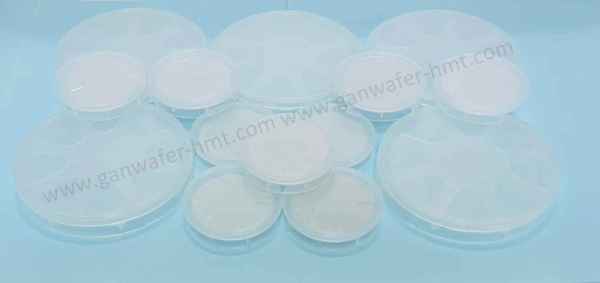
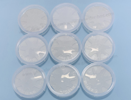
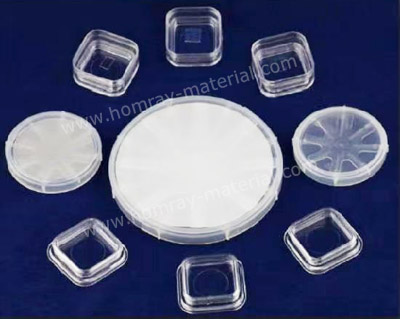
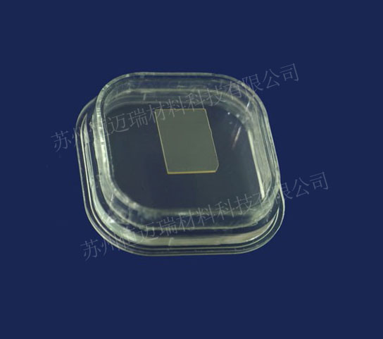
Related Products
![]() M.P: +86-15366208370 ; +86-15366203573
M.P: +86-15366208370 ; +86-15366203573
![]() E-mail: kim@homray-material.com;tina@homray-material.com
E-mail: kim@homray-material.com;tina@homray-material.com
HMT Silicon Carbide (SiC) Wafer Website: www.sicwafer-hmt.com