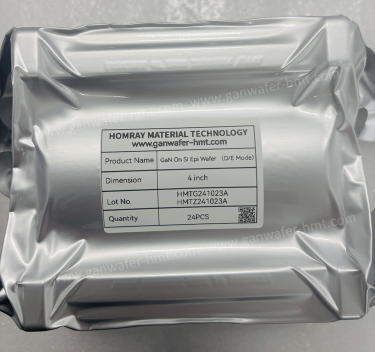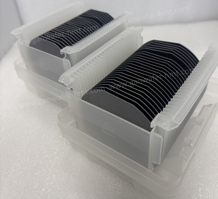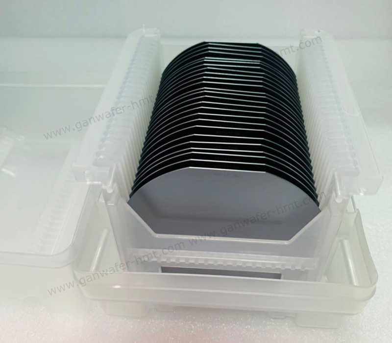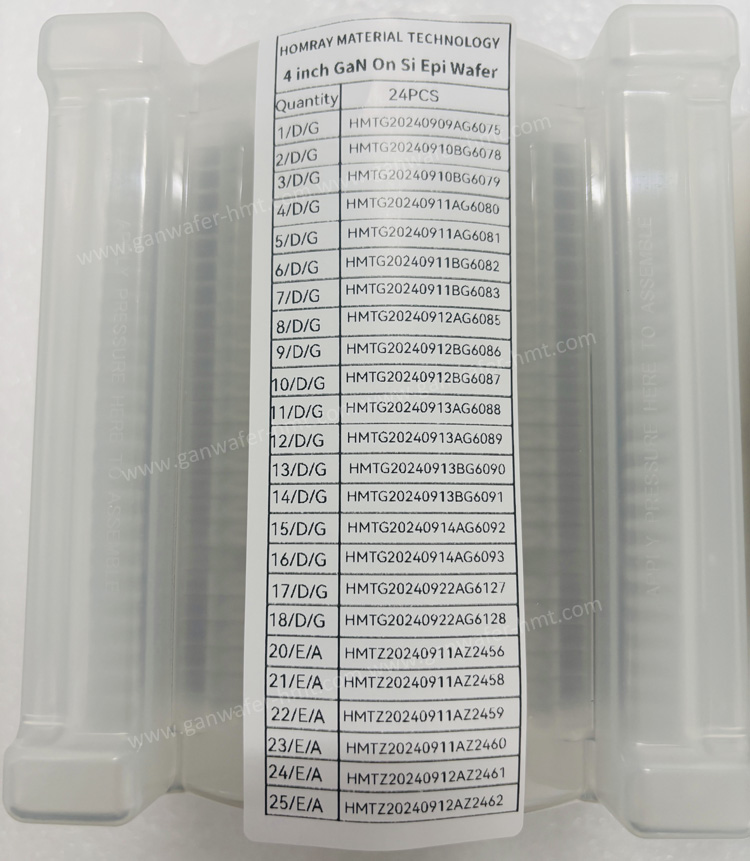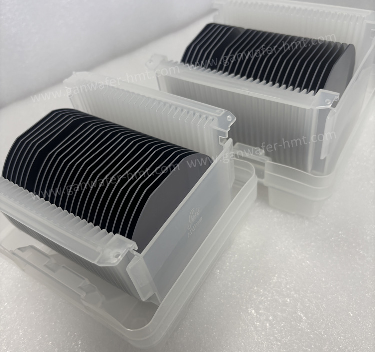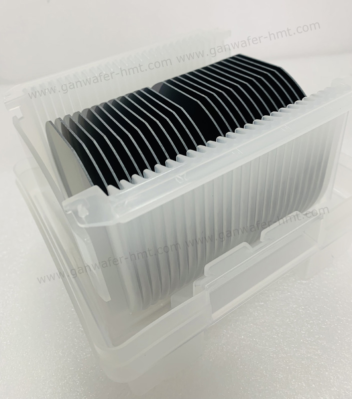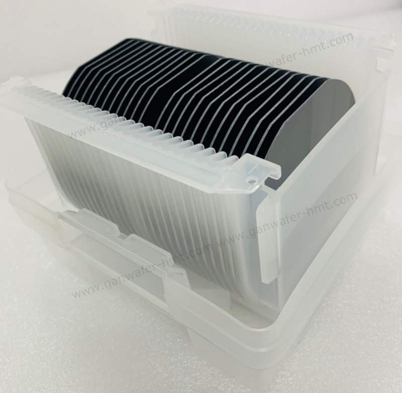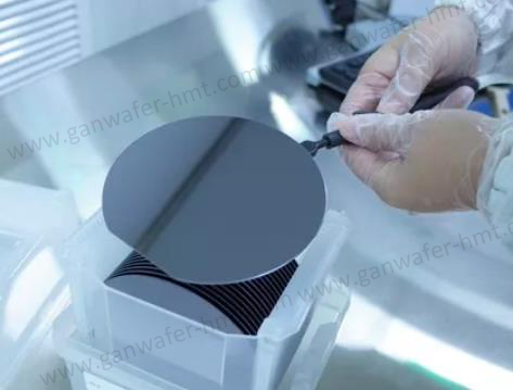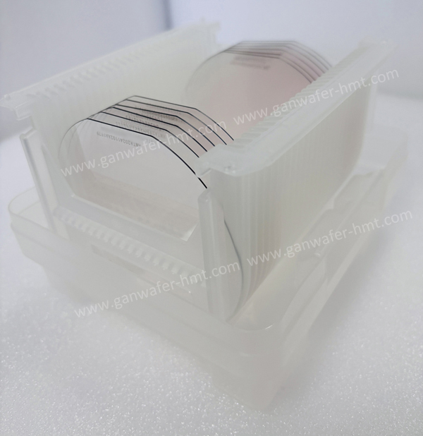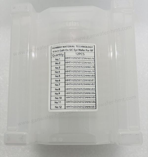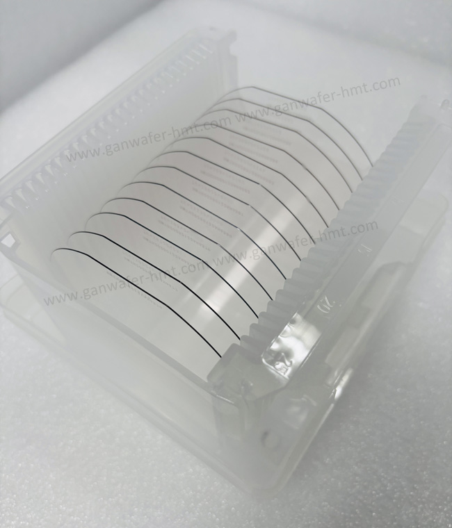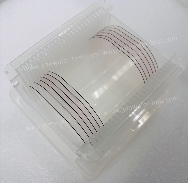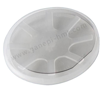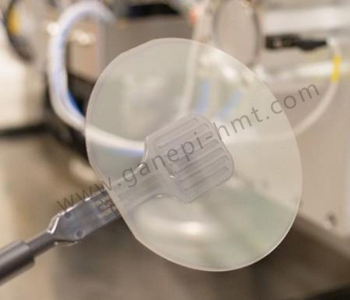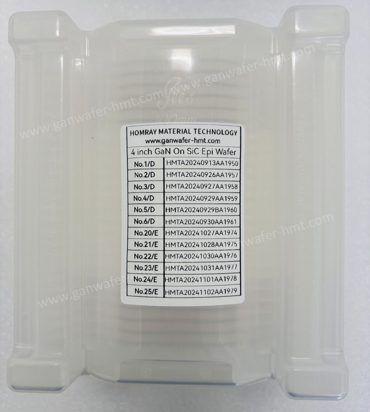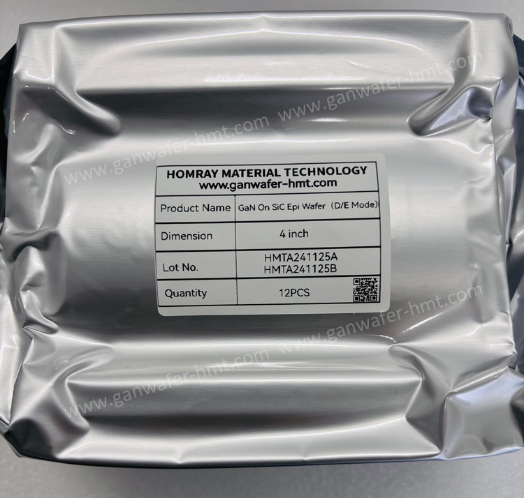
E-HEMT GaN on Si Epi Wafer Manufacturer
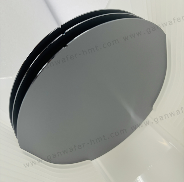
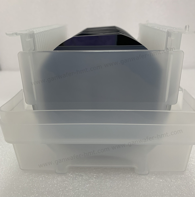
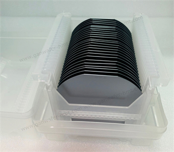
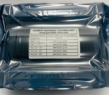
GaN-On-Si Epi Wafer For Power HEMT-E Mode
Substrate Diameter: 4-8 inch(111)
Substrate Thickness: 675,1000um
Epi Layer Total Thickness: 2~5.5um
Product Description
Homray Material Technology provides high-performance and high-quality GaN HEMT epitaxial wafers, including GaN-on-Si Epi wafer with Power HEMT E-mode and D-mode. We supply 2 inch,4inch,6inch,8inch GaN-on-Si Epitaxial Wafer with favourable price on the market in China. Silicon thickness is 675um and 1000um. Customized structure and layer parameters are available jin HMT company.
Benefits of using GaN
- High power
- High frequency
- High power efficiency
- Low power consumption, energy saving
- High-temperature robustness
- Exceed the limitations of current Si power device
Standard Layer Specification For Power HEMT E-Mode
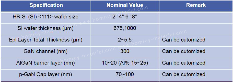
Characterization Specification

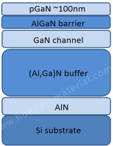
Standard Layer Structure
Related Products
