
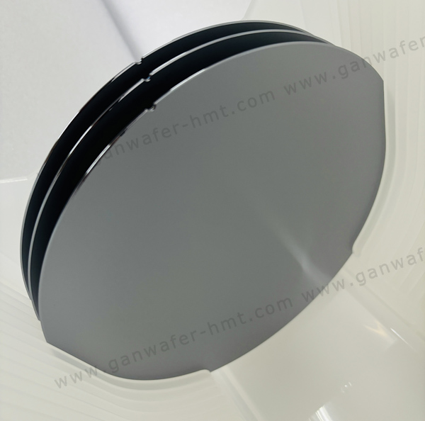
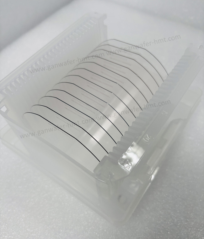
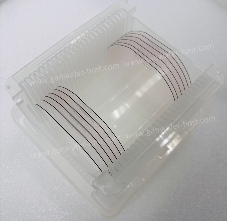
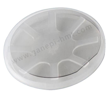
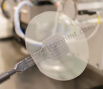
8 inch GaN-on-Si Epitaxy Wafer Manufacturer
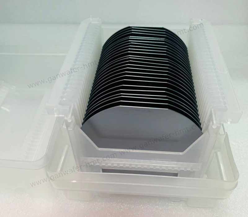
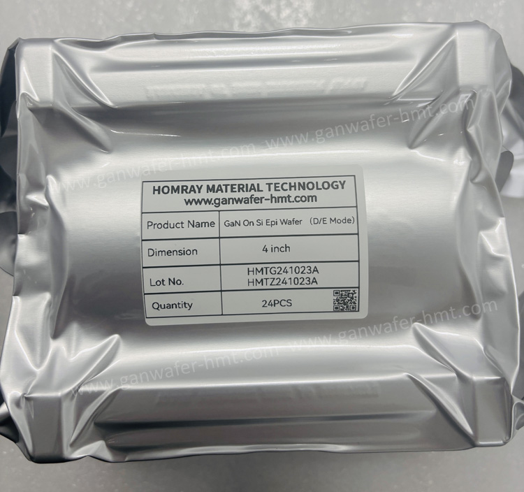
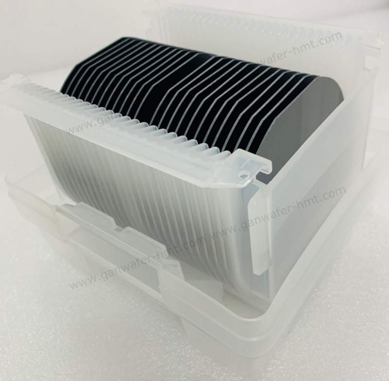
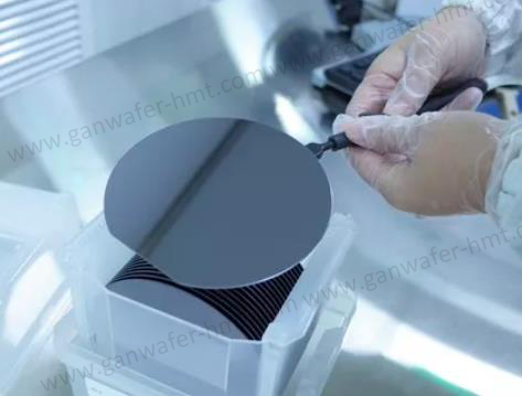
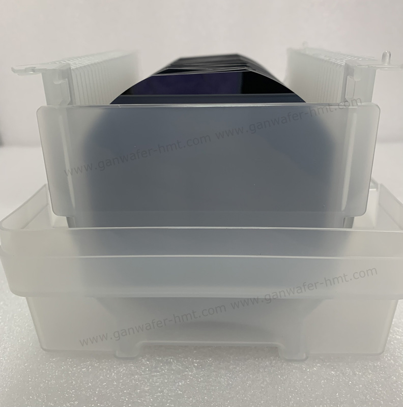
GaN-On-Si Epi Wafer
Substrate Size: 8 inch
Substrate Thickness: 1000um
GaN Buffer Layer: 2-3um
Product Description
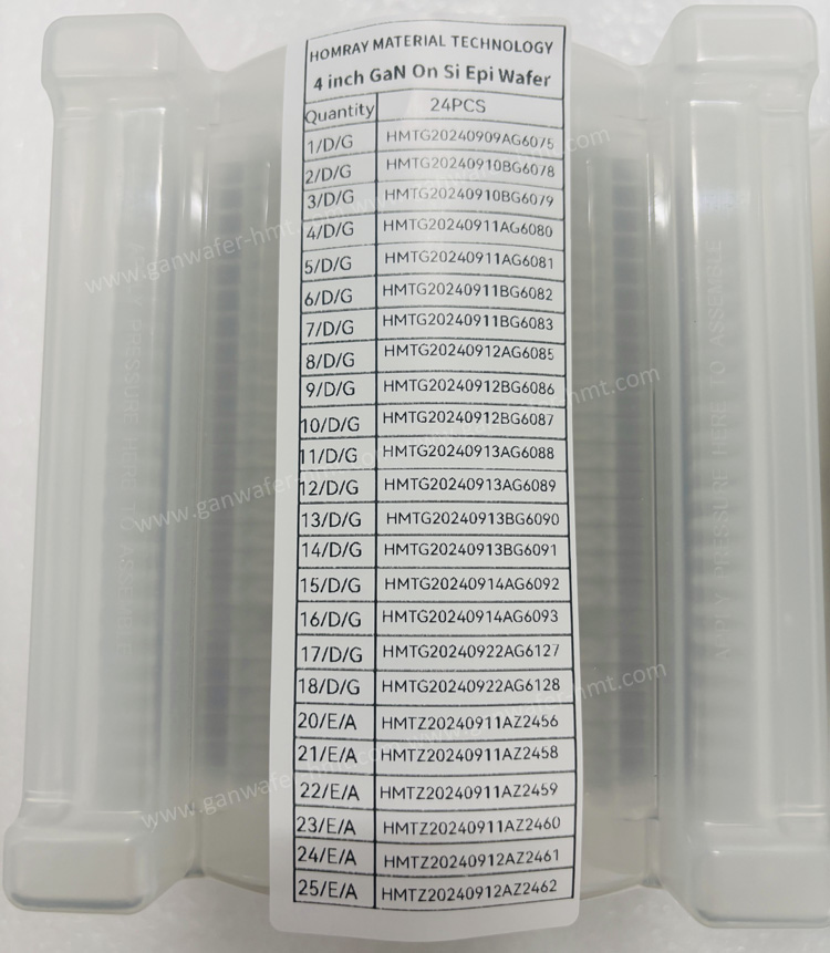
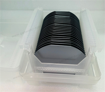
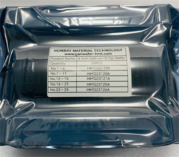
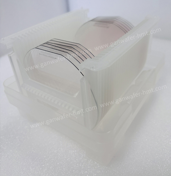
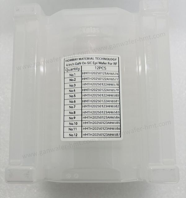
The main sizes of GaN-on-Si Epi wafer manufacturer and supplier by Homray Material Technology are 4 inch, 6 inch and 8 inch. GaN-on-Si power electronic devices and radio-frequency HEMT epitaxial sheets. The products have extremely high electron mobility and very small buffer layer leakage.Excellent epitaxial growth technology and good quality control ability ensure the uniformity and consistency of epitaxial material mass production.
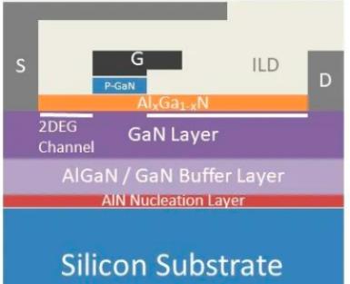
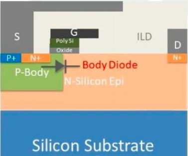
GaN HEMT Compare With Si LDMOS
GaN HEMT is based on AlGaN/GaN heterojunction, there is no GaN MOSFETs on the market at present, mainly because the cost of homogeneous GaN is too high, generally use Si or SiC as a heterogeneous substrate, heterogeneous substrate needs to grow a layer of buffer layer (AlN) on the substrate, and the buffer layer is insulating.
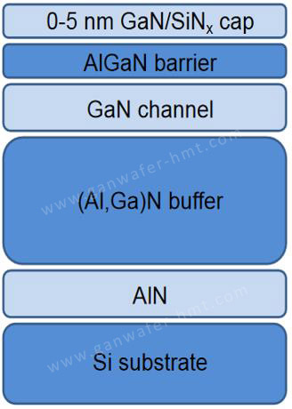
GaN-on-Si Epi Wafer Structure

Application of GaN in Driverless Technology
LiDAR uses laser pulses to quickly form three-dimensional images or create electronic maps of the surrounding environment. Gallium nitride field-effect transistors switch up to ten times faster than MOSFET devices, giving LiDAR systems advantages such as superior resolution and faster reaction times, which drive greater accuracy due to superior switching.
These capabilities have led to the emergence of new and broader LiDAR applications, including real-time motion detection for video game applications, gesture-driven computers, and autonomous vehicles.
Related Products

![]() M.P: +86-15366208370 ; +86-15366203573
M.P: +86-15366208370 ; +86-15366203573
![]() E-mail: kim@homray-material.com;tina@homray-material.com
E-mail: kim@homray-material.com;tina@homray-material.com
HMT Silicon Carbide (SiC) Wafer Website: www.sicwafer-hmt.com