AlGaN/GaN On SiC HEMT Epi Wafer Manufacturer
GaN-On-SiC Epi Wafer
Substrate Size: 4 inch,6 inch
Substrate Thickness:500um
Substrate Type: 4H-SI
Product Description
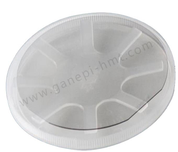
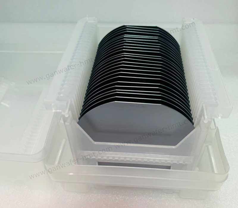
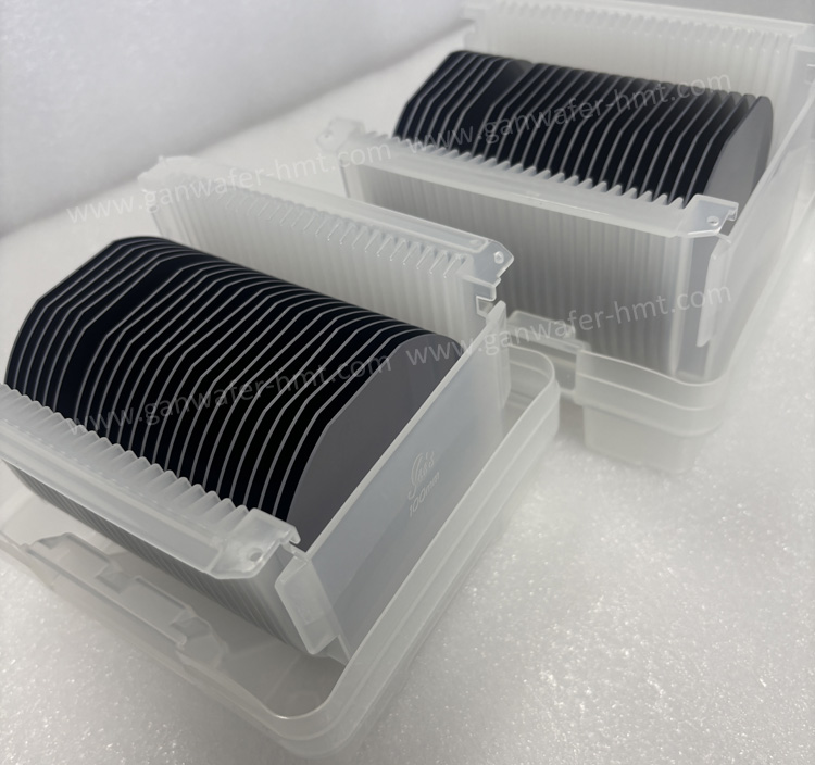
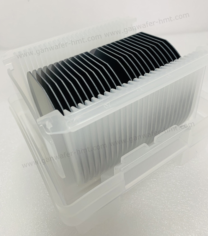
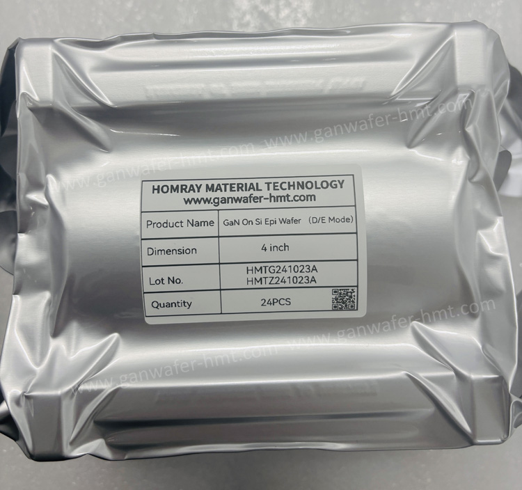
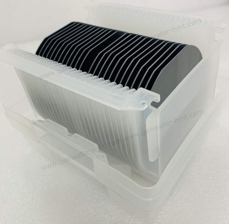
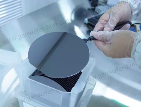
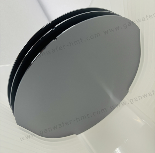
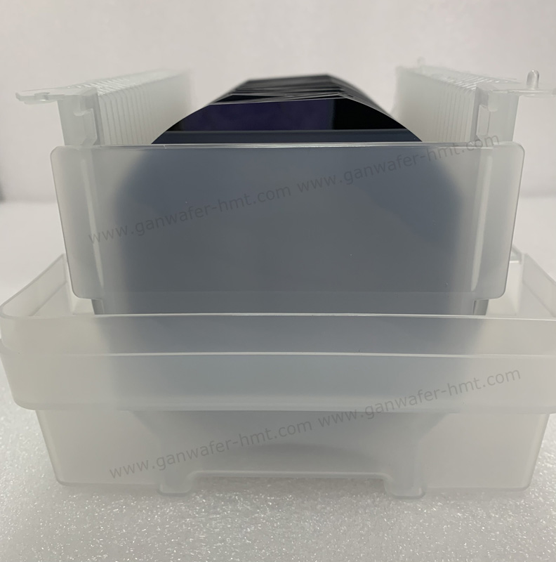
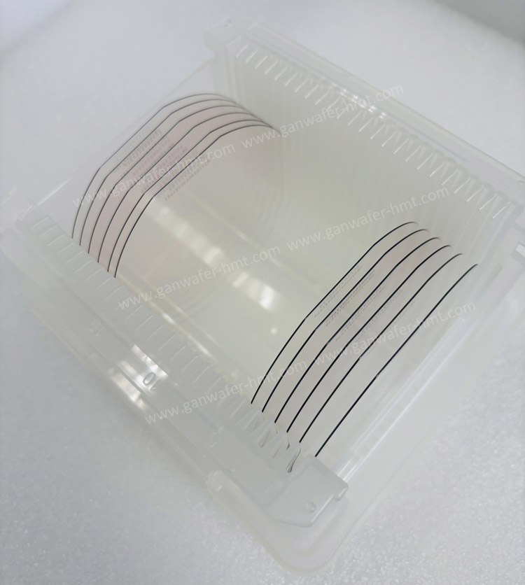
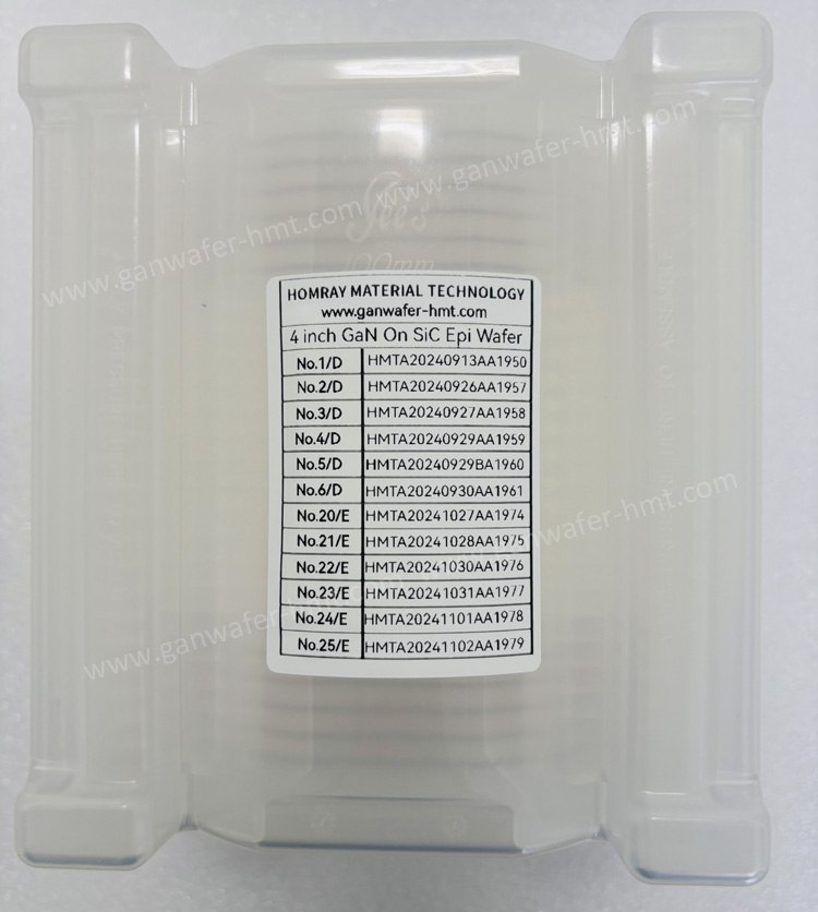
HMT company manufacture and supply 4inch AlGaN/GaN On SiC HEMT Epi wafers. GaN-on-SiC combines excellent thermal conductivity of SiC with high power density and low loss capability of GaN. The device on the substrate can operate at high voltage and high drain current. At present, the substrate of most GaN RF devices is silicon carbide. Limited to SiC substrates, our current supply of mainstream sizes of 4 inches and 6 inches, GaN-on-SiC epitaxial wafers are mainly used in the manufacture of microwave RF devices.
AlGan/GaN On SiC HEMT Epi Wafer Structure
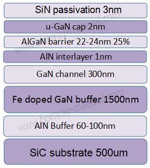
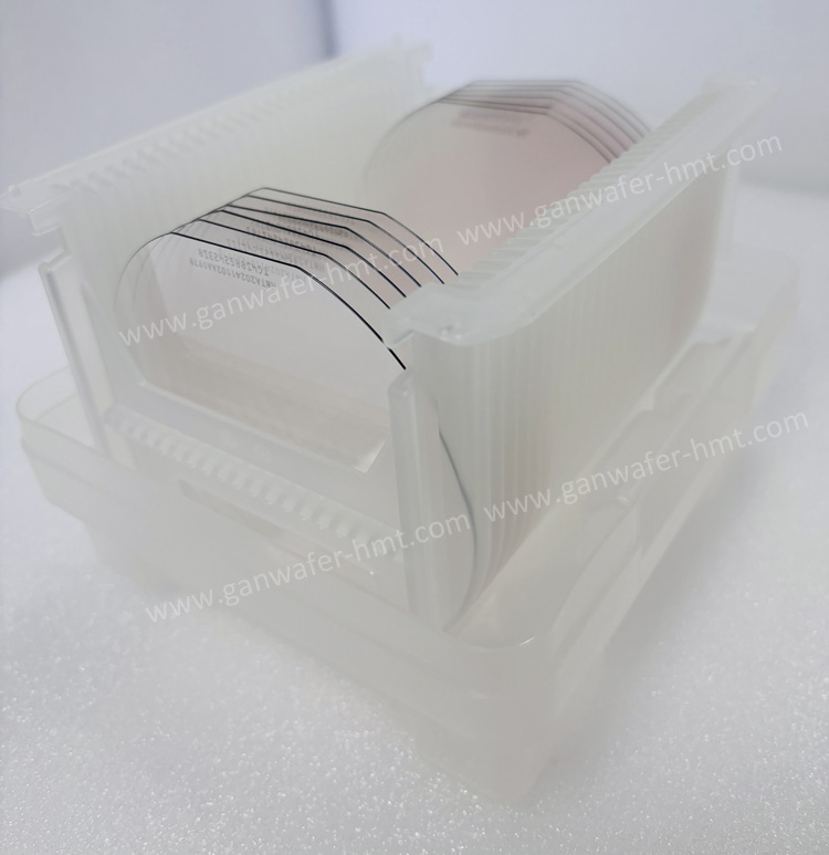
As the third generation semiconductor material, GaN has the advantages of high temperature resistance, high compatibility, high thermal conductivity and wide band gap. According to different substrate materials, gallium nitride epitaxial sheets can be divided into four categories: GaN on GaN, GaN on SiC,GaN on Sapphire and GaN on Silicon. Gallium nitride epitaxial chips are mainly used in the manufacture of electronic components, such as transistors, integrated circuits, and optoelectronic devices. It can improve the performance of electronic components, improve the reliability of components, and extend the service life of components.
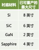
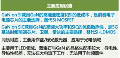
Advantages of several main substrates

Related Products
